This section introduces a number of useful digital logic chips for use in a
variety of projects.
Along the way I'll also cover some additional chip characteristics that can
be useful in complex designs.
The 74LS00 family
We've already spent time looking at the 7400 TTL logic family, even though I
only introduced the first part in the family.
The 7400 series was very successful and very popular, to the extent that when
companies want to manufacture new logic parts with different electrical
characteristics, they typically create new families of the very same functions
and pin-outs.
For example, the 7400 quad two-input NAND gate chip, with the pin-out we
presented earlier, has been reproduced with differing electrical
characteristics as the 74S00, 74LS00, 74S00, 74ALS00, 74AS00, 74F00, 74HC00,
74HCT00, 74AC00, 74ACT00, 74AHC00, 74AHCT, 74LV00, 74LVC00, and 74ALVC00, to
name a few.
There are some other 7400 family offshoots; this list is those flavors of
7400 currently in production from one manufacturer, Texas
Instruments.
For a long time, the original 7400 series was the best choice as a
general-purpose logic family, and the 7400 family had more members than any
of the offshoot families.
However, if you were picking a single "best" logic family today it
would probably have to be the 74LS00 family.
This family arguably has the widest manufacturer support and range of
available line of components.
The 74LS00 family improves technically on the 7400 family in two key areas:
faster speed and lower power consumption.
The only limitation of the 74LS00 family compared to the 7400 family is that
the 74LS00 family can only source half as much current.
However part of the current reduction in the 74LS00 family was on inputs,
such that a typical 74LS00 family part can drive twenty LS loads (that is,
one output can fan out to twenty inputs within the 74LS00 family; compare
this to the 7400 family, which could only drive ten inputs in the same
family).
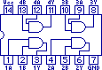
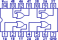
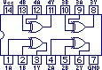
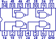
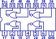
Two-input logic gates
The five standard two-input logic gates in the 74LS00 family are listed in
the table below.
Note that the pin-out for the 74LS02 (NOR gate) is inconsistent with the other
chips shown.
74LS08
AND
|
74LS32
OR
|
74LS86
XOR
|
74LS00
NAND
|
74LS02
NOR
|
Inverter
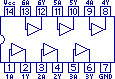
The basic inverter gate is the 74LS04.
There are six of these on a single chip.
74LS04
Inverter
|
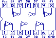
Open-collector gates
Many of the basic logic functions are also available in parts with "open
collector" outputs.
This is a modified output circuit within the chip which sinks current to
indicate a logic "0," but turns off to indicate a logic
"1."
These outputs do not source current.
These can be used in cases where the final output of a logic function only
needs to sink current; a later section will give examples where this can be
used.
Open collector gates have an interesting property, which is that they can be
ANDed together just by wiring several outputs together.
Ordinarily this is a Bad Thing because outputs could drive into each other, but
for open collector it's fine: any output being low causes a path to ground,
and multiple paths to ground are not a problem.
If all outputs are off, the combination of signals is also off.
(Since open collector is often used where "0" is the active state,
this is also called a "wired-OR" connection, referring to an
active-low OR function.)
74LS09
AND
|
|
74LS136
XOR
|
74LS07
Buffer
|
74LS38
NAND
|
74LS33
NOR
|
|
74LS05
Inverter
|
Tri-state buffers
Since a regular TTL logic gate sources current for "1" and sinks
current for "0," a signal where neither of these is happening (the
signal is "off," like in open collector outputs) can actually be
thought of as being a third state.
Parts which are capable of having their output in any of these three states
are considered to have "tri-state" outputs.
Tri-state outputs allow multiple gates to "take turns" driving an
output signal.
You might signal a logic function to drive its output (high or low as the
function may determine), and then later tell that function to turn off its
output so that a different function may drive the signal instead.
As long as other logic determines that no more than one output is driving the
same signal at the same time, all is well.
This method of combining multiple outputs on the same signal path is used
heavily in microprocessor circuits, where several different memory or input
circuits may be sharing a common set of data signals.
A tri-state buffer or inverting buffer looks like a regular buffer or
inverter, except there is an additional "enable" control signal
entering the gate.
When the enable is "1" the buffer is driving the output; when the
enable is "0," the output is turned off ("tri-stated").
Because tri-state buffers have many applications in microprocessor circuits,
there are several useful chips available which are designed to function on
eight data signals (bits) at one time.
74LS541
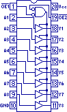
|
74LS540
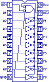
|
74LS245
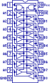
| In |
|
| /OE | DIR | Function |
| 1 | X | N.C. |
| 0 | 0 | B A A |
| 0 | 1 | AB |
|
The truth tables for the 74LS541 and 74LS540 introduce a new symbol,
"Z," which represents the "off" state.
(The correct term for this is "high-impedance," often shortened
to "high-Z.")
For the 74LS245 it would be more accurate to call it a "function
table," since it represents not the outputs but the functions performed
for different states at the /OE and DIR inputs.
The eight-bit buffers (74LS541 and 74LS540) are functionally equivalent to the
widely used 74LS244 and 74LS240; however the '244 and '240 have a more
confusing pin-out to trip the unwary student.
Latches
The 74LS573 is an eight-bit transparent latch, while the 74LS574 is an
eight-bit edge-triggered latch.
Each has an output enable pin that can tri-state all the outputs.
These chips have convenient pin-outs separating the input side from the
output side.
74LS573
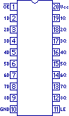
| In |
Out |
| /OE | LE | D | Q |
| 0 | 1 | 1 | 1 |
| 0 | 1 | 0 | 0 |
| 0 | 0 | X | Q0 |
| 1 | X | X | Z |
|
74LS574
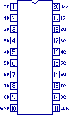
| In |
Out |
| /OE | CLK | D | Q |
| 0 |  | 1 | 1 |
| 0 | | 0 | 0 |
| 0 | 0 | X | Q0 |
| 1 | X | X | Z |
|
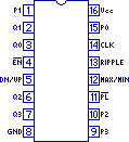
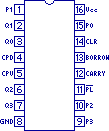
Counters
These four-bit counter parts can count up or down.
Outputs Q0 through Q3 are a binary value, where Q0 is the least signifigant
bit and Q3 is most significant.
An asynchronous preset allows the outputs to be latched to inputs P0 through
P3 when /PL is "0."
These counters change value on a clock transition from "0" to
"1."
The 74LS191 has a single clock input; the DN/UP input determines the meaning,
where a "1" causes the count to decrease or a "0" causes
the count to increase.
A separate /EN input has to be "0" or the clock is ignored.
A RIPPLE output can clock another stage counter for the next four bits.
A MAX/MIN output is set to "1" when Q0-Q3 show the count before
an overflow or underflow; that is, when DN/UP is "1" MAX/MIN
indicates "1" when the value is 1111 (binary) and when DN/UP is
"0" MAX/MIN indicates "1" when the value is 0000.
The 74LS193 has separate clocks for up (CPU) and down (CPD), and separate
outputs for CARRY and BORROW to clock the next stage.
There is a CLR input to reset the counter to 0000.
74LS191
|
74LS193
|
Although less common, there are decimal versions of these chips.
The 74LS190 is identical to the 74LS191 except it only counts from 0 through
9 (0000 through 1001 binary); the 74LS192 is similarly identical to the
74LS193 except for the limited range.
You might use these variants if you want to count in decimal digits rather
than pure binary.
There are plenty of other useful chips in the 74LS00 logic family, but these
are some of the most useful building blocks.
At the very least, they provide you with a lot of different options for
creating complex logic functions and circuits.
Next: Schematics and Components
Previous: Data Sheets
Copyright ©2003-2006, Mark Bereit. All rights reserved.
|