We've discussed logic gates, the basic building blocks for manipulating logic levels.
In this section we'll introduce registers, the basic building blocks for
storing data.
Remembering a bit
By combining logic gates you can perform various manipulations on logic
levels.
The states "flow" through gates from inputs to outputs.
It would stand to reason, then, that if you feed the output of a logic
function back into an input of that function, then the logic states will
endlessly flow through the function.
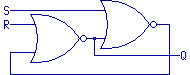
Consider this logic diagram:
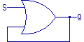
Suppose that both inputs were initially "0."
The output of the OR gate would be "0," which would feed back into
the gate, in an endless loop of "0."
Further suppose you subsequently set the first input, called "S" for
"set," to "1."
This would suddenly cause the output of the OR gate to become "1,"
which would feed back into the gate in an endless loop of "1."
However, any further changes to "S" would have no effect: the
output "Q" will stay at "1" no matter what.
The function "remembers" the "1" state.
With this function, we have for the first time introduced the dimension of
time into the logic.
Any logic function's output can change when its inputs change, but now there
is the additional consideration of what the inputs were before.
Notice also that a truth table, as we've described them so far, is
unable to describe this function, because a "0" input may
yield a "0" or a "1" for the output depending upon
whether the input was a "1" at some prior time.
There are also two practical problems with this function.
First, how do we know that the feedback state was initially
"0," when there is no way to input that state?
And second, once we set the function to a "1," how do we ever reset
it back to "0?"
For both of these problems, we need some way to reset the function before it
can really be any help.
All we need to do, though, is add a bit more logic.
Rather than have the output feed straight back into the OR gate, we need a
way to break that path.
We want the feedback path to be "1" if the OR gate output is
"1," and we have not applied a "1" to a separate
"reset" input.
Our revised function looks like this:
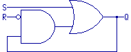
In this function we still don't know what state "Q" might be in
before we ever apply a "1" to the S (set) or R (reset) input,
but we know we can set it to whichever state we want and it will stay that
way.
A logic function like this, which can be set in either state by applying
different inputs, and then retain that state, is called a
"flip-flop."
The S-R flip-flop
The logic function we have just created is called an "S-R flip-flop,"
because inputs S and R set and reset (respectively) output Q.
(Calling a flip-flop output "Q" is another convention, like calling
the output of combinational logic "Y."
There may be good reasons for these choices of letters... but I don't know
what they are.)
However, if you look at an S-R flip-flop in a textbook, it doesn't look like
our function.
So before we talk about this flip-flop any further, let's make some adjustments
to our diagram.
First, we apply DeMorgan's theorem to turn the AND gate into another OR gate.
We changed the location of the inverters accordingly.
The end result is still the same logic function:
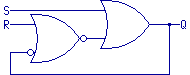
Next, we observe that while the flip-flop is holding a state, both gates'
outputs have the same state.
That is, the output of the right OR gate and the output of the left OR gate
(after the inverter dot) both represent the state of the flip-flop.
Thus we can move the output "Q" to the other gate without changing
its meaning.
This is a good point to mention that in logic diagrams, lines crossing over
each other do not indicate a connection.
When we want to indicate that lines connect, we use a filled dot at that
point.
This convention will also be used when we talk about schematic drawings later
in this course.
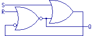
Anyway, now that we're not using the right gate's output as "Q"
any more, we are free to move the inverter dot off of the input to the left
OR gate, and onto the output of the right OR gate.
We'll invert the state of the connecting line, but otherwise the function
is unchanged.
Now we'll simply reposition the gates and lines, to better show the symmetry
we ended up with:
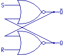
In this drawing, we also added a name for the other output: this time
"Q" with a bar above the letter.
In logic drawings and in digital electronics schematics, a bar over a name
indicates that the state represented by the name is true when the logic level
is "0."
In our flip-flop, the output of the lower NOR gate is "1" when the
flip-flop is "set," while the output of the upper NOR gate is
"1" when the flip-flop is "reset."
By convention, when a name is intended to convey a meaning (such as
"S" for "set") we expect that a "1" at that
point represents that meaning, but when the name has an overbar, then we
instead expect that a "0" represents that meaning.
For text where you can't draw a bar over a name (including the text
within this web site!), the same convention is often represented by a
slash before the name, as in "/Q" for the upper output.
Anyway, our drawing of the S-R flip-flop is now symmetrical, and looks like
you would find it in a textbook.
It's a logic function which can be set into either a "set" or
"reset" state, and stay in that state until it is changed.
However it is worth pointing out two peculiarities of this function.
First, as we mentioned before, there is no telling which state the function
is in before the first "1" is applied to either the set or reset
input; actually it is a characteristic of any flip-flop or logic
register to require some explicit reset before its state can be predictable.
And secondly, if you were to apply a "1" to both the set and reset
inputs at the same time, you would have the curious intermediate case where
both Q and /Q were "0," until either the set or reset returned to
"0" and the other input would prevail.
The simple solution to that situation is: don't do that.
If you never set both signals at the same time you don't have to worry about
it.
(If the larger logic functions in which you were using a flip-flop contained
the risk of both being true at once, you could use additional logic to not
allow the less-important input to be "1" if the more-important input
were "1.")
Here's the truth table for our S-R flip-flop function:
| in | out |
|---|
| S | R | Q | /Q |
|---|
| 0 | 0 | Q0 | /Q0 |
| 0 | 1 | 0 | 1 |
| 1 | 0 | 1 | 0 |
| 1 | 1 | 0 | 0 |
You see that the states of Q and /Q are described in this table not as specific
logic levels but as the prior values of Q and /Q.
The subscripted "0" represents the "original" or
"prior" state of that name.
The transparent latch
The S-R flip-flop works great for "registering" which of two logic
inputs was "1" most recently.
However in digital electronics we more often want to register what logic level
was present at a particular input at some previous point in time.
Consider this more complex flip-flop:
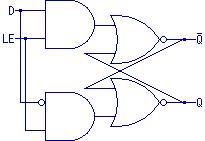
In this function we have made a data input "D" which gets set into
the flip-flop only when a latch enable input, "LE," is high.
If the D input changes while LE is "1," the flip-flop follows that
state "transparently," but at the time when the LE input goes to
"0," the flip-flop is "latched" in the last state that
was seen on D.
Here's the truth table:
| in | out |
|---|
| D | LE | Q | /Q |
|---|
| X | 0 | Q0 | /Q0 |
| 0 | 1 | 0 | 1 |
| 1 | 1 | 1 | 0 |
As with the S-R flip-flop, there are other ways of diagramming this function
(some of which yield better circuit implementations).
But the function of a transparent latch is a useful concept.
The edge-triggered latch
The transparent latch had two modes of behavior: when the LE input was
"1," the output followed the input, and when the LE input was
"0," the output ignored the input.
But you could say that the "latch" operation occurred right at the
transition from "1" to "0."
Another type of latch, arguably the most important in digital logic, is the
edge-triggered latch, where a transition is the only time the output can
change.
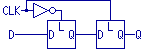
Consider this diagram, combining two transparent latch functions back-to-back:
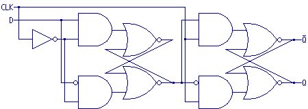
The data input feeds into the first transparent latch.
Another input, "CLK," is inverted and used as the latch enable for
the first transparent latch.
That is, the output of the first transparent latch follows the input when
CLK is "0" and latches the data value when CLK transitions to
"1."
The second transparent latch accepts data from the first transparent latch,
but this latch gets CLK without being inverted.
So the same time that the first latch is freezing the data value is when the
second latch "accepts" the first latch's data.
The overall effect is that when CLK goes from "0" to "1,"
the function latches the data input as the Q output, and at no other time
can the output change.
We need to add still another notation to our truth tables to represent this
function:
| in | out |
|---|
| D | CLK | Q | /Q |
|---|
| 0 |  | 0 | 1 |
| 1 | | 1 | 0 |
| X | 0 | Q0 | /Q0 |
| X | 1 | Q0 | /Q0 |
The up-arrow symbol
""
means "rising edge," although that term may not mean anything to
you until we discuss timing diagrams later in this course.
But it simply indicates that point in time when the logic level
"rises" from a "0" to a "1."
(As you might guess, a transition from "1" to "0" is
called a "falling edge.")
The truth table tells us that the rising edge is the only time when anything
happens in this function.
Function blocks
Now, suppose that we want to represent the logic to latch two eight-bit values
from a common set of inputs at two discrete rising-edge signals, and perform a
binary "OR" merge on those bits to yield another eight-bit value.
We could draw a diagram with all those gates... but on second thought, let's
not!
Even though we now know all the pieces that make up this function, it would
still be a large, complex and redundant diagram containing 152 gates.
If you are already familiar with computer programming, our use of the term
"function" may already lead you to the next point, which is that once
you have a logic function that works a certain way (such as an edge-triggered
latch), you can shortcut the diagram by simply indicating uses of that function
rather than draw out the logic every time.
Just like a computer program function lets you define a function once but lets
you call that function (or someone else's function) any number of times, a
logic diagram can replace a block of logic with a simple box that indicates the
use of some more complex logic function.
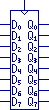
Consider these two symbols:
| Transparent | Edge-triggered |
 |
 |
The first of these could represent the transparent latch.
We've reduced it to the two inputs, data and latch enable, and a single output
"Q."
If we needed the /Q output it could be added to the box as well.
The point is, we've replaced the implementation of the logic function (the
diagram of the four gates earlier in this page) with a simple box representing
an instance of that function.
The second diagram is a representation of the edge-triggered latch.
It looks almost the same, except the CLK input is now denoted by a triangle
into the box.
That's another one of those conventions we keep mentioning; this one always
indicates an edge-triggered input, and since this function only has one
edge-triggered input there is no need to give it a label.
How do you know what particular function is represented by the box?
You simply give it a label, like "transparent latch," so you know
what it is.
There's no special syntax involved; after all, this is all (so far) just
diagrams to help us understand the logic we're representing.
The use of boxes for logic functions is just a way of simplifying our
diagrams.
After all, it would have been simpler if we had presented the edge-triggered
flip-flop with a diagram like this:
As long as you understand that the two blocks are the transparent latches we
discussed previously, the diagram conveys the same meaning a lot more simply.
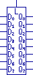
There is an additional simplification we use in logic diagrams.
When you want to represent a set of identical function blocks sharing some
common signal(s), you can simply extend the block to make room for the
signals not repeated. Consider these two symbols:
| Transparent | Edge-triggered |
 |
 |
These blocks represent eight bits of transparent latch or edge-triggered latch,
all eight bits sharing a common latch enable or clock input.
Common signals appear on the ends that aren't stretched, while repeated signals
appear on the ends that are stretched.
Subscripts after the names indicate individual instances (here bits 0 through
7) and let you match the elements from a particular block.
We understand that this box represents eight instances of the specific function
block.
For a combined function block like these, there is no value to creating a
truth table with every combination of "1" and "0" for the
various data inputs.
We can simply indicate that the behavior of any one input and output follows
for all, as in this example for the combined edge-triggered latch:
| in | out |
|---|
| Dn | CLK | Qn |
|---|
| 0 | | 0 |
| 1 | | 1 |
| X | 0 | Q0 |
| X | 1 | Q0 |
Counters
The edge-triggered latch can easily be turned into a toggle function, by
feeding the negative output (/Q) back into the data input, like this:

Every time the clock input transitions from "0" to "1,"
the output goes to the opposite state.
Now suppose we combined several of these toggle functions, back to back:
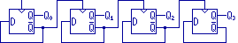
Every time one of the outputs changes from "1" to "0,"
the inverted output changes from "0" to "1," which
drives the next stage to change states.
We have effectively built a logic function that counts in binary.
Consider this state machine for the transitions:
| in | previous | out |
|---|
| CLK | Q3 | Q2 | Q1 | Q0 |
Q3 | Q2 | Q1 | Q0 |
|---|
| 0 | 0 | 0 | 0 | 0 | 0 | 0 | 1 |
| 0 | 0 | 0 | 1 | 0 | 0 | 1 | 0 |
| 0 | 0 | 1 | 0 | 0 | 0 | 1 | 1 |
| 0 | 0 | 1 | 1 | 0 | 1 | 0 | 0 |
| 0 | 1 | 0 | 0 | 0 | 1 | 0 | 1 |
| 0 | 1 | 0 | 1 | 0 | 1 | 1 | 0 |
| 0 | 1 | 1 | 0 | 0 | 1 | 1 | 1 |
| 0 | 1 | 1 | 1 | 1 | 0 | 0 | 0 |
| 1 | 0 | 0 | 0 | 1 | 0 | 0 | 1 |
| 1 | 0 | 0 | 1 | 1 | 0 | 1 | 0 |
| 1 | 0 | 1 | 0 | 1 | 0 | 1 | 1 |
| 1 | 0 | 1 | 1 | 1 | 1 | 0 | 0 |
| 1 | 1 | 0 | 0 | 1 | 1 | 0 | 1 |
| 1 | 1 | 0 | 1 | 1 | 1 | 1 | 0 |
| 1 | 1 | 1 | 0 | 1 | 1 | 1 | 1 |
| 1 | 1 | 1 | 1 | 0 | 0 | 0 | 0 |
| 0 | X | X | X | X | Q0 | Q0 | Q0 | Q0 |
| 1 | X | X | X | X | Q0 | Q0 | Q0 | Q0 |
A counter is another function block which is usually represented as a simple
box rather than as its component latches or gates.
Our four-bit counter above could be represented like this:

Of course, we can just as easily extend this function to any number of bits,
because we know how to combine the basic building blocks to make any size we
want...and knowing that, we don't need to draw it every time.
...We could spend a lot more time discussing registers and logic blocks and the
kinds of complex functions we can build by putting these pieces together,
but you get the basic idea.
It's time to put the concepts into practice.
In the next section we'll start to look at actually building circuits using
digital logic chips.
Next: Logic Chips
Previous: Logic Gates
Copyright ©2003-2006, Mark Bereit. All rights reserved.
|